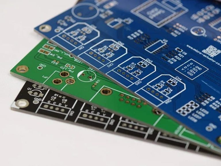

PCB design services can prove to be surprisingly difficult to achieve, particularly when under tight deadlines, complicated circuit needs, and pressure to launch sooner. Perhaps you have attempted untrustworthy freelancers, confusing tools, or outdated services.
If so, you’re likely asking yourself: Can there be a more efficient method of handling PCB board design without compromising quality or speed? The good news: there is. In this article, we present you with LHD’s online PCB design services, created to make your development easier, wiser, and more trustworthy.
No matter if you’re beginning with zero or require high-end multilayer board support, we’ll guide you through the ways that LHD can assist in turning your ideas into reality, professionally and with online collaboration convenience.
So, let’s get started.
Why PCB Design Matters More Than Ever?
Previously, the design of the printed circuit board was viewed as an ordinary part of product design, technical, yet not necessarily differentiating. No longer. With electronics getting smaller, faster, and more intelligent, PCB design is now one of the principal drivers of product performance, reliability, and success.
Here are the reasons why designing your PCB board correctly is more important than ever:
1. Devices Are Shrinking, But Power Is Growing
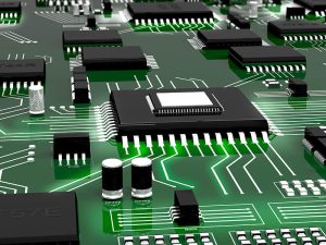
From smartphones to Internet of Things (IoT) wearables, modern devices are shrinking in size, yet not at the sacrifice of performance. This makes them require extremely dense and accurate PCB layouts. More and more designers need to pack more parts, connections, and functionality into confined spaces—frequently on multi-layer or HDI structures.
One single routing mistake or ill-placed component can result in overheating, signal loss, or even equipment malfunction. Professional PCB design, then, is not just beneficial—it’s essential.
2. High-Speed Signals Demand High-Precision Layouts
With higher data speeds and high-frequency components, signal integrity is no longer an option but an imperative. Careless trace design can induce crosstalk, electromagnetic interference (EMI), or timing problems, which are notoriously difficult to debug after the board is built.
Good PCB design incorporates these into consideration through methods such as impedance control, differential pair routing, and meticulous ground plane planning. This makes the signal flow stable and device operation smooth, even at high frequencies.
3. Regulatory Compliance Is Tougher Than Ever
EMC (Electromagnetic Compatibility), FCC, CE, and RoHS are strict regulatory standards and are being enforced ever more frequently. Bad PCB layout can create radiated emissions or susceptibility problems that make products fail compliance testing, leading to costly redesign, production delay, or legal issues.
Having an experienced design team working with you guarantees your board not only meets your needs but is compliant right from the outset, both saving you time and money.
4. Thermal Management Can Make or Break Your Product
The more power they contain and the faster the processors, the more critical it becomes to manage heat. A board with an ill-suited layout can overheat or fail prematurely, even with a good schematic.
Today’s PCB design services do more than simply lay out electronics—components are placed strategically, with thermal vias, heat sinks, and copper pours to remove heat effectively. This keeps performance high while prolonging the lifecycle of your product.
5. Manufacturing Success Starts at the Design Level
Most PCB problems do not appear until manufacturing time. Pad sizes, violation of spacings, or untestable designs can cause failed builds, reduced yields, or complete production stops.
It’s why modern PCB design incorporates Design for Manufacturability — or DFM. Experts know the manufacturing and assembly process and create according to it, minimizing the potential for costly mistakes in production.
6. Time-to-Market Pressure Is Real
In today’s high-speed markets, being first is more critical than being perfect. Yet, hurrying the design of the PCB can prove to be an ordeal. Mistakes in the layout stage can take weeks, or even months, to rectify down the line.
With our expert online PCB design services, you have the advantage of quick turnaround times without sacrificing quality. This equates to fewer delays, smoother prototypes, and getting to market sooner.
7. Increasing Complexity Needs Collaborative Tools
No single engineer builds modern electronics these days—these are team efforts. So, there’s an immediate need for PCB design to be easy to work with, review, and hand over to others. As design becomes more intricate, older offline methods simply can’t keep up.
Online PCB design comes into play here, with real-time feedback, cloud-based versioning, and smooth communication among design teams, engineers, and decision-makers.
8. The Cost of Rework Is Higher Than Ever
One little design flaw can create an avalanche of problems—overdue deadlines, failed prototypes, and cost overruns. Even worse, when an errant board goes into production, recall costs and damage to reputation can prove overwhelming.
Professional-level PCB design enables you to “get it right the first time.” With simulations, validation checks, and expert guidance, a good design keeps rework to an absolute minimum and brings you peace of mind.
The LHD Advantage in PCB Design
LHD is not just a PCBA manufacturer—we are your single-source online partner for all of your PCBA design needs. From the first schematic capture to the end layout optimization, we provide complete solutions end-to-end that are tailored for performance, manufacturing, and cost-effectiveness.
What makes LHD unique is:
1. Expert Engineering Team
Our skilled PCB designers and electrical engineers are experts in high-speed, multi-layer, and high-complexity circuit design. Whether designing an industrial control board or a compact wearable, our team can assist you in making the right decision at each step, from component positioning to trace routing.
2. Seamless Online Collaboration
There’s no need to be in the same time zone—or even the same city—to work with us. Your online PCB design workflow is designed with real-time communication, secure file exchange, and open project tracking. You’re kept informed with frequent updates, proofs, and revisions, all via our online interface.
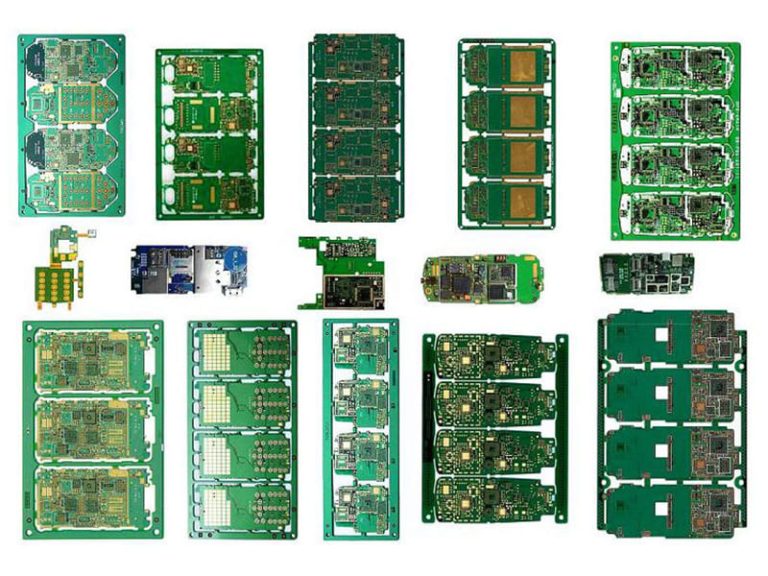
3. Multi-Layer and High-Speed PCB Capabilities
We specialize in:
- Multi-layer stack-up designs (up to 32+ layers)
- High-Frequency Layout for RF and Microwave Applications
- Differential pair and impedance-controlled routing
- Blind, buried, and via-in-pad technology
- EMI-conscious design principles
4. DFM, DFA & DFT Integration
LHD’s PCB board design strategy isn’t solely about functionality—it’s also about Design for Test (DFT), Design for Assembly (DFA), and Design for Manufacturability (DFM). Through our process, we make certain that your end product is streamlined for efficient, cost-conscious manufacturing and effortless testing, minimizing time to market and the likelihood of failure.
Our Online PCB Design Process

At LHD, we feel that good design comes from starting with an explicit, step-by-step methodology. This is how our online services for designing PCBs operate:
Step 1: Requirement Gathering
We start with an understanding of your project’s purpose, performance needs, and technical requirements. You’re requested to provide component listings, mechanical constraints, and schematic files, where they exist.
Step 2: Design Proposal & Timeline
After reviewing your input, we present an in-depth design proposal with scope, cost, approximate turnaround time, and critical project milestones. Your expectations are clearly outlined before we get started.
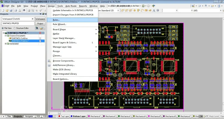
Step 3: Schematic Capture
Our designers employ tools such as Altium Designer, Cadence Allegro, and KiCad to record circuit diagrams. Each component and each connection is fully checked to ascertain accuracy and compatibility.
Step 4: PCB Layout Design
This is where the magic begins. We begin to route your board, being careful to adhere to industry standards for trace width, trace spacing, signal integrity, and thermal management.
Step 5: Review & Approval
Layout proofs and 3D visuals are provided to you for checking. Any required alterations are dealt with immediately prior to sign-off.
Step 6: Gerber File & Output Generation
After approval, we create manufacturing files (Gerbers, drill files, BOM, etc.) and documentation required for production.
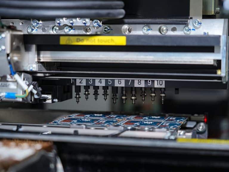
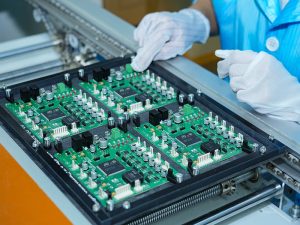
Step 7: Optional Fabrication & Assembly
Need your design turned into an actual product? LHD also provides fabrication, component procurement, and assembly to offer a total turnkey solution.
Tools & Software We Support
To maintain compatibility and adaptability, we use an assortment of commonly used software tools:
- Altium Designer
- OrCAD / Cadence Allegro
- Mentor Graphics PADS
- Zuken CR-8000
We also support file conversions and cross-platform integrations if you’re switching design platforms mid-project.
Industries We Serve
Our board design services are relied upon by businesses in several high-demand industries, which are:
- Consumer Electronics: Smartphones, wearables, IoT devices
- Industrial Automation: Control systems, robotics, sensors
- Automotive Electronics: ECUs, power management systems
- Medical Devices: Diagnostic equipment, portable monitors
- Telecom and Networking: Routers, signal boosters, fiber transceivers
- Aerospace & Defense: Avionics, navigation units, radar systems
Common Challenges We Help You Solve
Our clients are usually coming to us with one or more of the following problems:
- Unclear signal paths or crosstalk issues
- EMI/EMC failures during regulatory testing
- Poor thermal management
- Incompatible layout for mass manufacturing
- Delays caused by rework or communication with the designer
Our task is to remove all the headaches, starting from the very beginning.
Why Online PCB Design Services Are the Future
The electronics engineering world keeps changing at an accelerating pace, and old-school design methodologies are beginning to show their age. Email threads, file compatibility issues, and endless meetings can hold innovation back and drive unnecessary expense. That’s why growing numbers of businesses are leveraging cloud-based online PCB design services—a faster, cheaper, and more team-friendly method that harmonizes with the needs of contemporary engineering.
- Quicker Turnaround with Digital-First Processes
In a competitive marketplace, each hour matters. Internet-based PCB design services cut through the bottlenecks inherent in manual methods. No waiting to see physical design prints or scheduling in-office reviews—every step takes place in real time. Files can be uploaded, reviewed for design revisions, and authorized from anywhere, which significantly speeds up the development phase.
No matter if you’re designing prototypes or moving into high-volume production, speed is important, and staying digital keeps your PCB project in motion.
- Seamless Teamwork Across Teams and Time Zones
Modern product development is not often siloed. All of the following need to have access to the same design files: product managers, electrical designers, manufacturing teams, and hardware engineers, and they need to stay synchronized. Online platforms for PCB provide common dashboards, version control, and real-time editing, so distributed teams can work together easily without duplicating effort or getting confused.
By having everyone operate from one source of truth, you eliminate miscommunication and enhance design integrity.
- Complete Visibility and Real-Time Transparency
Weary of chasing email notifications or waiting days for feedback about your design? Online systems give you instant visibility into the progress of your project. With an online PCB design portal, for instance, clients are able to see the current status of their boards, post feedback, approve revisions, and see milestones all in one area.
Transparency creates trust, keeps all the stakeholders informed, and facilitates the progress of the project without friction.
- Lower Costs and Reduced Overhead
Traditional workflows for PCBs have underlying costs—numerous rounds of editing, printed prototypes, eleventh-hour mistakes, and repeated rounds of feedback. Online tools eliminate these costs to a great extent by simplifying communication, automating the exchange of files, and minimizing the likelihood of errors.
Additionally, many Internet-based services, such as LHDs, provide built-in tools for DFM (Design for Manufacturability) verification, Gerber checking, and thermal simulation, all under one roof. Fewer errors, quicker approval, and reduced time and money invested in time-consuming revisions.
- Scalability and Flexibility Through Built-In
No matter whether you’re an early-stage startup creating your initial prototype or an established company expanding production, online PCB design services offer you the flexibility to scale up without reaching operational ceilings. You can begin with just several design files and scale all the way up to full-stack development, from testing to assembly and quality assurance, all under one platform.
No need to spend money on costly infrastructure or implement new tools. The platform expands with your business.
- Convenient Availability of Expertise
An additional benefit of online services? You are never alone. Through our online design system, at LHD, you’re in direct contact with trained engineers and project managers. Whether you need assistance with layout optimization, component procurement, or technical verification, professional help is just an instant message away.
This access keeps you right on track, even as your designs become more intricate.
Conclusion: Select LHD for Reliable Online PCB Design
If your project is too critical to entrust to luck, team with an organization that makes your success their own. LHD’s printed board design services combine technical know-how, state-of-the-art tools, and an efficient online workflow to take you from idea to product, free from the typical frustration and delays.
No matter if you are an OEM expanding production or starting your initial prototype as a startup, LHD offers flexibility, expertise, and dependability to aid in your experience.