
HDI board problems holding your project back? Don’t worry, you’re not alone. Engineers and product designers everywhere have difficulty locating dependable manufacturing partners who can produce high-performance boards with the space and speed needs that are required today.
Poor quality, missed production timelines, or insufficient customization can ruin even the greatest ideas. Worry not, though; this article is here to aid you.
We’re here to guide you through all you need to know about selecting a professional custom HDI PCB producer that delivers right the first time. If you’re after clarity, confidence, and actual solutions, you’re with the right people.
So, let’s get started.
What Is HDI PCB?
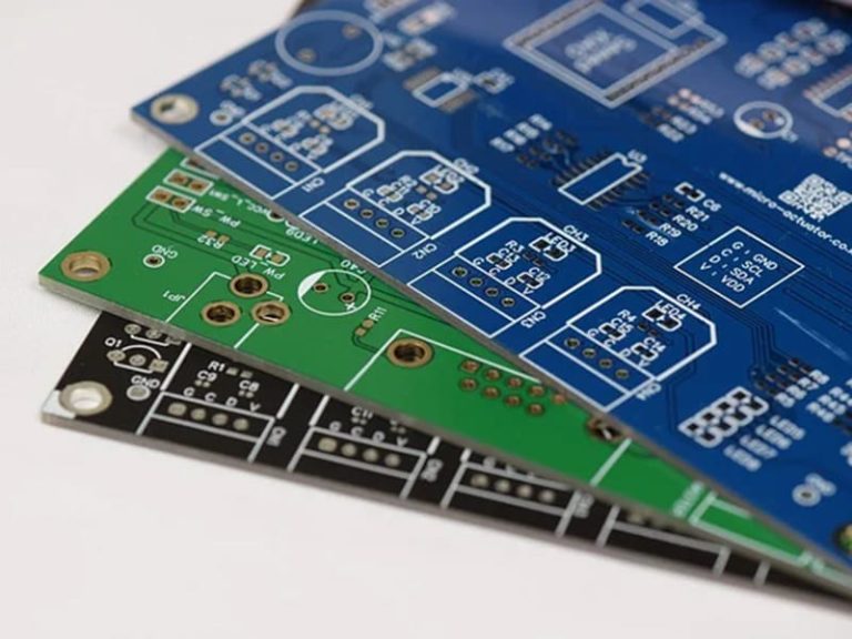
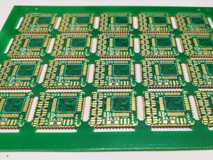
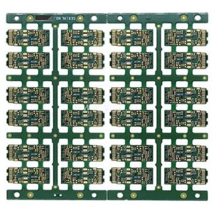
High-Density Interconnect (HDI) Printed Circuit Boards are sophisticated printed circuit boards with higher wiring density, which enables more parts to fit in a reduced space when compared to standard PCBs. HDI technology employs microvias, fine lines, and layers to raise board interconnectivity, which effectively supports more functionality in a more compact design.
This is essential for applications requiring high performance and compact form factors, which include, for example, mobile phones, medical devices, car electronics, and consumer electronics.
Key Characteristics of HDI PCBs
HDI PCBs are distinct from common PCBs in many respects, especially when it comes to manufacturing and design complexity.
The essential features are:
Fine-Line Traces and Microvias
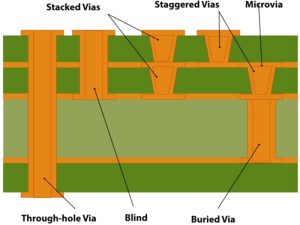
One of the characteristic features of HDI PCBs is microvias, or very small, accurately drilled holes, which connect the layers of the PCB. Microvias enable more and denser traces, minimizing the size of the PCB but maximizing its functionality.
They also improve the board’s electrical performance by minimizing signal loss and interference. Larger vias in traditional PCBs occupy more space and cause signal degradation. Microvias enable HDI PCBs to have higher precision and performance even in very tight spaces.
Multilayer Stacking
HDI PCBs commonly have several layers stacked upon one another. These multilayer boards make cost-effective routing of traces possible and improve the overall performance of the PCB. The layers may range from 4 to 12 layers or more, depending upon the design’s level of complexity as well as the needs of the application.
Layer stacking makes HDI PCBs more flexible and adaptable to many applications, from straightforward consumer products to specialized automotive or medical equipment.
Smaller Form Factor
With the worldwide trend towards shrinking the size of electronics, HDI PCBs prove to be the best solution. HDI PCBs make it possible to develop high-speed devices with small sizes.
In applications such as wearable technology and smartphones, the demand for small but high-performance PCBs becomes imperative. HDI technology enables manufacturers to pack more parts into fewer spaces, allowing sleeker, more efficient products to be created.
Key Features of HDI PCBs
There are several characteristics that make HDI PCBs the go-to choice for many high-performance applications.
Higher Component Density
HDI PCBs are made to support higher component densities than regular PCBs. This makes it possible to add more components into the same or even reduced footprint, enabling the manufacturing of more complicated circuits.
The need to pack more parts into an ever-decreasing space is critical in areas such as telecommunications, where space is limited, yet performance must not be sacrificed.
Microvia Technology
The application of microvias in HDI PCBs has real performance and design benefits. Microvias are laser-drilled and are substantially smaller compared to the traditional via. These small vias enable improved routing among the layers in the PCB and decrease the size of the overall board.
The end result is an improved, more compact design with maximum performance. This is particularly relevant for high-speed applications, where impedance and signal degradation are minimized with fewer via sizes.
Multilayer Designs
HDI PCBs can have several layers, enabling more complicated circuits to be created. HDI boards aid in both signal routing and interlayer connections, enhancing both performance and flexibility.
With the use of several layers, manufacturers are able to route power, ground, and signal traces for optimal performance, minimizing interference while enhancing signal integrity.
Fine Traces and Small Pads
The higher accuracy of HDI PCBs enables the use of more precise traces and narrower pads, which increase the board’s electrical performance. Efficient use of space is facilitated with fine traces, while minimal pads prevent signal loss.
This is critical for high-speed circuits, where performance is reliant upon minimizing the component-to-component distances and minimizing resistance.
Improved Electrical Performance
These HDI PCBs have excellent electrical performance. Due to the microvia technology and fine traces, these boards are able to manage high-frequency signals more effectively. Fewer signal paths, decreased impedance, and the removal of unnecessary elements are the reasons behind the high electrical performance of HDI boards.
These are well-suited for usage in products like smartphones, networking devices, and other high-speed devices.
The Benefits of Choosing a Professional Custom HDI PCB Manufacturer
When choosing an HDI PCB producer, it is essential to do business with an organization that offers both experience and cutting-edge technology.
The following are the main advantages of working with an expert HDI PCB maker:
Customization to Meet Specific Needs
Each project is different, be it the size of the PCB, layers, or the features required for the function of the application. A professional HDI PCB maker can provide customization according to these requirements.
By employing a company that can provide custom-made solutions, you can have the confidence that the PCB can perfectly fit into your device, which can range from an embedded smartphone to an intricate industrial device.
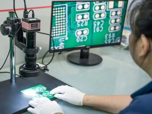
Quality Control and Testing
Reliability and durability of electronics are guaranteed with high-quality HDI PCBs. A professional PCBA manufacturer would maintain strict quality control standards so that each board is always conforming to the standards of the industry.
The testing methods can involve Automated Optical Inspection (AOI), X-ray inspection, and electrical testing to detect possible defects prior to shipping the board. This type of testing is essential in guaranteeing the performance and reliability of HDI PCBs.
Expert Engineering Support
Professional HDI PCBA manufacturers also have engineering support to aid in design and HDI PCB development. If you need guidance in optimizing the layout or selecting the best materials for your application, an experienced team of engineers can provide valuable insights to ensure that the design is cost-effective and efficient.
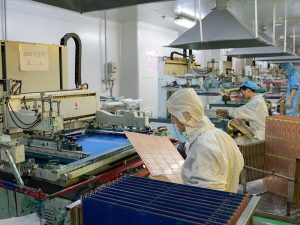
Advanced Manufacturing Technology
In order to make high-quality HDI PCBs, a firm needs to have modern manufacturing technologies at its disposal. These consist of sophisticated drilling technology, precision machinery, and cutting-edge testing equipment.
Such an able manufacturer would commit to these technologies to provide HDI PCBs of the highest quality and performance standards.
Reduced Time-to-Market
Time-to-market is an important consideration in today’s competitive business environment. Having an efficient HDI PCB producer who has optimized production can minimize lead times, with the result that your product can hit the shelves sooner.
This is especially the case in industries where technology develops quickly, for example, consumer electronics and telecommunications.
Why HDI PCBs Are Crucial for Modern Electronics?
The significance of HDI PCBs cannot be overemphasized in present-day electronics. HDI PCBs provide the critical support necessary to make the miniaturization and high-performance characteristics of modern devices possible.
The following are some of the reasons why HDI PCBs are necessary in the design of modern electronics.
Miniaturization of Devices
The growing trend of miniaturizing electronics makes HDI PCBs the ideal choice. HDI PCBs make it possible for manufacturers to develop higher-powered products in compact sizes.
From smartphones to wearables to medical devices, HDI PCBs provide the miniaturization needed while ensuring high functionality.
High-Speed Applications
HDI PCBs are especially preferred for applications requiring high speeds, such as 5G devices, network devices, and gaming consoles. HDI boards with their fine traces and short signal paths ensure minimal loss of signal, which makes them best suited for devices with high data transfer speeds.
Enhanced Performance and Reliability
HDI technology improves both the performance and reliability of devices. Through minimizing signal interference and sustaining peak electrical integrity, HDI PCBs make sure that electronic devices function effectively under changing circumstances.
This is particularly critical in applications where failure is unacceptable, like medical devices or car safety systems.
Support for Complex Designs
Most contemporary electronics need sophisticated circuitry with intricate layouts and multi-layer structures. HDI PCBs offer the space and flexibility to support these kinds of layouts with high performance.
It’s particularly important in industries such as telecommunications and aerospace, where reliability and performance are essential.
Choosing the Right HDI PCB Manufacturer
Finding the best HDI PCB manufacturer is not simply about comparing prices—it’s about identifying a proven partner who is knowledgeable about high-density interconnect technology and can provide consistent performance. When you’re making this critical decision, here are the critical factors you need to consider:
1. Proven Experience and Technical Expertise
Experience makes all the difference, particularly with something as critical as HDI PCB manufacturing. Use an HDI board manufacturing company with plenty of experience producing HDI boards for many different applications, ranging from consumer products to space systems. A firm with decades of experience under its belt won’t simply go through your design; it’ll predict issues, recommend improvements, and guide you towards performance, cost, and manufacturing optimization.
An expert team can also assist you with engineering consultations, stack-up design advice, and layout optimization—factors that can make or break a high-speed, high-density board.
2. Advanced Manufacturing Capabilities
Not all manufacturers are capable of meeting the challenge of HDI technology. Check for factories that are equipped with leading-edge machinery, like laser drilling equipment, high-resolution image systems, automated plating lines, and cleanrooms. These are the technologies needed to manufacture the fine features, microvias, and multilayer stack-ups necessary in HDI designs.
More sophisticated configurations can further accommodate sequential lamination, via-in-pad plating, and laser direct imaging—factors that are indispensable for realizing HDI PCBs that are high-performance, robust, and compact.
3. Rigorous Quality Control Processes
Nothing is more important than quality assurance. Your reliable HDI PCB supplier must have a documented, multi-stage quality control policy that addresses all stages of manufacturing. Request information about their inspection procedures, including Automated Optical Inspection, X-ray inspection, electrical testing, and microsection analysis.
Also, verify for global certifications such as ISO 9001, UL, RoHS, or IPC Class 3 standards. These certifications prove that the supplier is meeting high standards of quality and environmental compliance, providing you with extra assurance that your boards will function effectively in actual applications.
4. Transparent Communication and Reliable Customer Support
Regardless of how excellent the equipment of a company may be, communication problems can spoil the project. The good manufacturer needs to behave like a real business associate—offering frequent feedback, identifying potential problems beforehand, and responding promptly to your questions or issues.
From initial design files to finished shipment, your manufacturing partner needs to have someone available to guide you through each step. Some of the best partners have dedicated project managers or engineers committed to your account, so your needs are not forgotten.
LHD Technology: A Leading HDI PCB Manufacturer
LHD Technology Co., Ltd. is a leading custom HDI PCB provider, with industries covering consumer electronics, medical devices, and more. For over twenty years, LHD Technology has excelled in manufacturing PCBs with uncompromising quality, cutting-edge technology, and outstanding customer support.
Why Choose LHD Technology?
- Customization: With LHD Technology, we provide customized solutions for HDI PCBs, ensuring your precise needs are achieved.
- State-of-the-Art Equipment: LHD employs cutting-edge machinery to create high-performance HDI PCBs with high reliability and quick turnaround times.
- Quality Assurance: All HDI PCBs are thoroughly tested to make sure they are of the highest standards and function dependably in challenging applications.
Conclusion
HDI PCBs are an essential technology for electronics in the modern age, allowing devices to shrink without compromising performance. When you work with an expert HDI PCB fabrication company such as LHD Technology, you can have confidence that your project will realize the best in terms of quality, dependability, and performance.
Whether you require an individualized solution for an end product in the consumer space or an intricate design for an industrial use, LHD Technology can provide the talent and capabilities required to make your vision happen.